
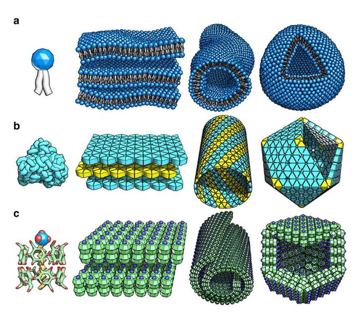
The field of nanotechnology has witnessed an explosion of research and development, leading to the creation of materials with unique and enhanced properties stemming from their nanoscale dimensions. Understanding the structure and composition of these nanomaterials is paramount for controlling their behavior and optimizing their performance in diverse applications, ranging from medicine and electronics to energy and catalysis. Among the arsenal of characterization techniques available, X-ray Diffraction (XRD) holds a prominent position. Its non-destructive nature and sensitivity to the long-range order within materials make it an invaluable tool for unraveling the intricacies of their crystalline structure. Here we explore the types of nanomaterials analyzed by XRD, the aspects it reveals, and its broader role in material research.
Why Use XRD Analysis for Nanomaterials
XRD analysis offers a unique window into the world of nanomaterials, providing insights that are often difficult or impossible to obtain with other techniques. At its core, XRD exploits the interaction of X-rays with the electron clouds of atoms arranged in a crystalline lattice. When a beam of monochromatic X-rays strikes a crystalline material, it is diffracted by the regularly spaced atomic planes according to Bragg’s Law (nλ=2dsinθ), where n is an integer, λ is the wavelength of the X-rays, d is the interplanar spacing, and θ is the angle of incidence. The resulting diffraction pattern, a plot of intensity versus diffraction angle (2θ), acts as a fingerprint of the material’s crystalline structure.
For nanomaterials, XRD analysis is particularly crucial because their properties are often strongly dependent on their size, shape, crystal structure, and phase purity. The technique allows researchers to identify the constituent phases, determine the average crystallite size, assess the degree of crystallinity, measure lattice parameters, and even gain insights into strain and defects within the nanoscale structure. The ability to obtain this fundamental structural information is essential for correlating synthesis parameters with material properties, understanding reaction mechanisms at the nanoscale, and ultimately designing nanomaterials with tailored functionalities. The non-destructive nature of XRD also allows for repeated measurements under different conditions (e.g., temperature, pressure) to study dynamic structural changes.
Types of Nanomaterials Analyzed by XRD
In the field of nanomaterials, X-ray diffraction (XRD) technology is widely used for in-depth analysis of the following six types of materials due to its high sensitivity to crystal structure:
1. Nanoparticles:
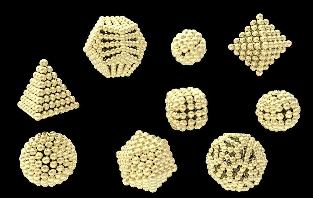
Nanoparticles, typically defined as particles with at least one dimension between 1 and 100 nanometers, are fundamental building blocks in nanotechnology. Their high surface area to volume ratio and quantum confinement effects often lead to unique physical and chemical properties.
XRD analysis for nanoparticles is primarily used to determine their phase identification and purity. By matching the observed diffraction peaks with reference patterns in databases like the International Centre for Diffraction Data (ICDD), the crystalline phases present in the nanoparticle sample can be identified, and the presence of any unwanted impurity phases can be detected. Furthermore, the average crystallite size of the nanoparticles can be estimated using the Scherrer equation (D= Kλ/βcosθ ), where D is the average crystallite size, K is a shape factor, λ is the X-ray wavelength, β is the full width at half maximum (FWHM) of a diffraction peak (in radians), and θ is the Bragg angle. For instance, a study on synthesized gold nanoparticles might show broadened XRD peaks compared to bulk gold, and applying the Scherrer equation to these peaks would yield an estimate of the average nanoparticle diameter.
XRD can also reveal information about the crystal structure (e.g., face-centered cubic for gold nanoparticles) and lattice parameters, which might slightly deviate from the bulk values due to surface effects or strain.
XRD provides crucial structural information about nanoparticles, enabling researchers to confirm the successful synthesis of the desired phase, estimate their size, and assess their crystalline quality.
2. Nanopowders:
Nanopowders are ensembles of individual nanoparticles. While each nanoparticle can be analyzed individually (with challenges for very small sizes), XRD on nanopowder samples provides a bulk average of the structural characteristics of the constituent nanoparticles.
Similar to individual nanoparticles, XRD analysis of nanopowders allows for phase identification and purity assessment of the bulk sample. The average crystallite size of the nanoparticles within the powder can be determined from the peak broadening. Additionally, XRD can provide information about the overall crystallinity of the nanopowder sample, indicating the relative amounts of crystalline and amorphous phases. The lattice parameters of the crystalline phases present can also be precisely determined. In cases where nanopowders undergo processing (e.g., sintering, annealing), XRD can be used to monitor phase transformations and changes in crystallite size as a function of the processing conditions. For example, researchers studying the thermal stability of a titania nanopowder might use XRD at different temperatures to observe any changes in the crystalline phase (e.g., anatase to rutile transformation) and the evolution of crystallite size.
XRD is an indispensable tool for characterizing nanopowders, providing essential information about their phase composition, average crystallite size, and overall crystalline nature. This bulk structural information is critical for controlling the properties and performance of nanopowders in various applications, such as catalysis, energy storage, and advanced ceramics.
3. Nanostructured Thin Films and Coatings:
Nanostructured thin films and coatings, where at least one dimension of the structural features is in the nanometer range, are crucial for applications in electronics, optics, and surface engineering. Their properties are highly dependent on their crystallographic orientation, phase composition, and internal strain.
XRD analysis of thin films and coatings goes beyond simple phase identification. Techniques like grazing incidence XRD (GIXRD) are employed to enhance the signal from the thin film while minimizing the contribution from the substrate. XRD can determine the phase composition of the film, identify any preferred crystallographic orientations (texture) using pole figure analysis, and assess the epitaxial quality of crystalline films grown on single-crystal substrates. By analyzing peak shifts and broadening, XRD can also be used to determine the residual stress and strain within the film. Furthermore, X-ray reflectivity (XRR), a related technique, can provide precise information about the film thickness, density, and interfacial roughness. For instance, in the development of transparent conductive oxides (TCOs) like aluminum-doped zinc oxide (AZO) thin films, XRD can confirm the formation of the desired hexagonal wurtzite structure, reveal the preferred orientation of the crystallites, and quantify the residual stress that can affect the film’s electrical conductivity.
XRD provides crucial information about phase composition, texture, epitaxial quality, residual stress, and even thickness, which are all critical factors influencing the performance of nanostructured thin films and coatings in their respective applications.
4. Nanowires and Nanotubes:
Nanowires (one-dimensional nanostructures with high aspect ratios) and nanotubes (hollow cylindrical nanostructures) exhibit unique electronic, optical, and mechanical properties due to their confined dimensions. Understanding their crystal structure and orientation is crucial for realizing their potential in nanoelectronics, sensors, and composite materials.

XRD analysis of nanowires and nanotubes can be challenging due to the often limited amount of material and potential preferred orientation within the sample. However, it can still provide valuable information about their crystal structure and phase purity. By carefully preparing aligned samples or using specialized sample holders, researchers can obtain diffraction patterns that reveal the dominant crystallographic planes and identify any secondary phases. The average crystallite size along the growth direction or within the walls of the nanotubes can be estimated from peak broadening. Furthermore, XRD can be used to determine the preferred orientation of the nanowires or nanotubes in a bulk sample, which can significantly impact their macroscopic properties. For example, XRD analysis of aligned carbon nanotubes might show a strong diffraction peak corresponding to the graphitic planes oriented parallel to the alignment direction.
While sample preparation can be more complex, XRD remains a valuable tool for characterizing the crystal structure, phase purity, crystallite size, and preferred orientation of nanowires and nanotubes.
5. Semiconductor Nanomaterials:
Semiconductor nanomaterials, including quantum dots, nanowires, and thin films made of semiconducting materials like silicon, germanium, and metal oxides, are at the heart of modern electronics and optoelectronics. Their size-dependent electronic and optical properties make precise structural characterization crucial.
XRD analysis plays a vital role in characterizing semiconductor nanomaterials by confirming the crystal structure (e.g., cubic zincblende for many II-VI and III-V semiconductors, diamond cubic for silicon and germanium) and phase purity. For quantum dots, while peak broadening can be significant due to their small size, XRD can still provide information about the overall crystal structure and estimate their average size. For semiconductor nanowires and thin films, XRD can determine the crystallographic orientation, assess the presence of defects (which can affect electronic properties), and measure strain in epitaxial layers. For instance, XRD analysis of a gallium nitride (GaN) thin film grown on sapphire can confirm the hexagonal wurtzite structure of GaN and reveal the presence of any strain at the interface, which can influence the performance of GaN-based LEDs.
XRD is an indispensable technique for characterizing the crystalline structure, phase purity, orientation, and defect structure of semiconductor nanomaterials. This detailed structural information is crucial for understanding and controlling their electronic and optical properties.
6. Nanocomposites:
Nanocomposites are multiphase materials where at least one phase has dimensions in the nanometer range. The combination of different nanoscale constituents often leads to synergistic properties that are superior to those of the individual components.
XRD analysis of nanocomposites is used to identify the crystalline phases of the individual nanomaterials and the matrix material. It can also help in detecting any new phases formed at the interfaces between the different components due to chemical reactions during processing. While directly quantifying the dispersion of nanoparticles within the matrix can be challenging with conventional XRD, changes in the intensity or broadening of the diffraction peaks of the nanofiller can provide indirect information about their distribution and interaction with the matrix. For example, in a polymer nanocomposite reinforced with carbon nanotubes, XRD can confirm the presence of the graphitic structure of the nanotubes and the crystalline phases of the polymer matrix. The absence of new peaks might suggest good compatibility and minimal interfacial reactions. XRD is a valuable tool for characterizing the phase composition and identifying potential interfacial reactions in nanocomposites.
To sum up, XRD is non-destructive (only 5-50 mg of sample is required for a single test) and high-throughput (10 samples can be scanned in full spectrum per hour) in nanomaterial analysis. However, it has low sensitivity to amorphous components (such as amorphous carbon) and needs to be combined with small-angle X-ray scattering (SAXS) or other techniques for comprehensive characterization.
To achieve a more comprehensive characterization of nanomaterials, XRD is often used in conjunction with other complementary techniques such as:
- Transmission Electron Microscopy (TEM): Provides real-space imaging of individual nanoparticles, their size, shape, and internal structure, including grain boundaries and defects.
- Scanning Electron Microscopy (SEM): Offers surface morphology information and can be coupled with Energy Dispersive X-ray Spectroscopy (EDS) for elemental analysis.
- Atomic Force Microscopy (AFM): Provides high-resolution surface topography and can measure mechanical properties at the nanoscale.
- Raman Spectroscopy: Sensitive to vibrational modes and can provide information about molecular structure, bonding, and phase identification, particularly for carbon-based nanomaterials.
- X-ray Photoelectron Spectroscopy (XPS): Provides information about the elemental composition and chemical states of the elements present on the surface of the nanomaterial.
Considerations When Choosing XRD Analysis for Nanomaterials:
Obtaining accurate and meaningful results from XRD analysis of nanomaterials requires careful consideration of several factors:
Crystallinity:
XRD relies on the diffraction of X-rays by the periodic arrangement of atoms in a crystalline lattice. Therefore, the degree of crystallinity of the nanomaterial significantly impacts the quality and interpretability of the XRD data.
Highly crystalline nanomaterials produce sharp, well-defined diffraction peaks, allowing for precise phase identification, lattice parameter determination, and crystallite size estimation. In contrast, amorphous or poorly crystalline nanomaterials yield broad, weak halos with limited discernible peaks, making detailed structural analysis challenging with conventional XRD. The presence of both crystalline and amorphous phases in a sample will result in a pattern with both sharp peaks and broad features. Quantifying the degree of crystallinity often involves comparing the integrated intensities of the crystalline peaks with the intensity of the amorphous halo. For instance, a polymer nanocomposite with well-dispersed crystalline nanoparticles will exhibit sharp diffraction peaks superimposed on a broader amorphous background from the polymer matrix.
Particle Size:
The size of the crystallites within a nanomaterial has a direct impact on the width of the diffraction peaks. This phenomenon forms the basis for crystallite size estimation using the Scherrer equation.
As the crystallite size decreases below approximately 100 nm, the diffraction peaks broaden. This broadening is inversely proportional to the crystallite size. For nanoparticles with very small crystallite sizes (below ~5 nm), the peaks can become extremely broad and weak, overlapping with the background and making accurate analysis challenging. In such cases, advanced data analysis techniques or complementary techniques with higher sensitivity to short-range order might be necessary. It’s important to note that the Scherrer equation provides an estimate of the average crystallite size, which may not always be the same as the physical particle size observed by techniques like electron microscopy, especially if the nanoparticles are polycrystalline. For example, a sample of 10 nm gold nanoparticles might exhibit XRD peaks corresponding to an average crystallite size of 8 nm, indicating the presence of grain boundaries within some of the nanoparticles.
Particle size, specifically the crystallite size, significantly affects the XRD pattern, particularly the peak broadening. While this broadening allows for crystallite size estimation, very small particle sizes can lead to challenges in data interpretation, necessitating careful analysis and potentially the use of complementary techniques.
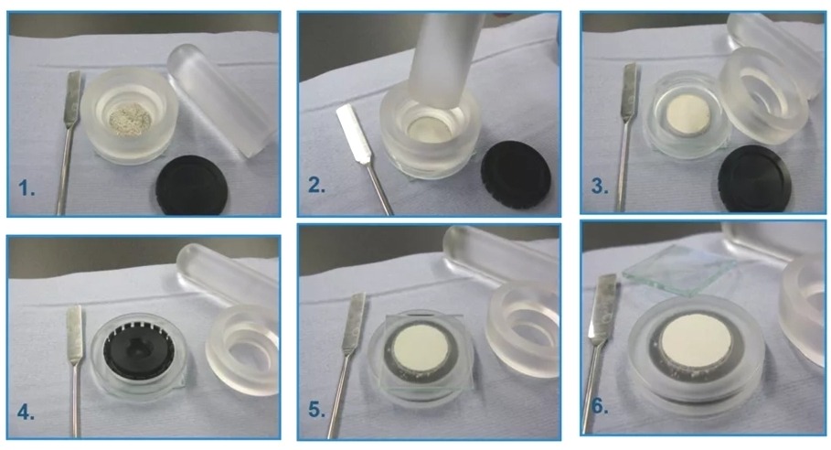
Sample Preparation:
Proper sample preparation is crucial for obtaining high-quality and representative XRD data from nanomaterials. Inadequate sample preparation can lead to artifacts and inaccurate results.
For nanopowders, it is essential to ensure a finely ground and randomly oriented sample to minimize preferred orientation effects, which can lead to inaccurate intensity measurements. The powder should be uniformly packed into the sample holder to ensure consistent X-ray interaction. For thin films and coatings, the sample should be flat and aligned correctly with the X-ray beam. For nanowires and nanotubes, special sample preparation techniques might be required to align them or concentrate them sufficiently to obtain a measurable signal. Contamination from sample handling or the sample holder itself should be avoided. For instance, if a nanopowder sample is not ground finely enough, larger agglomerates might lead to non-representative diffraction patterns. Similarly, a thin film sample that is not perfectly flat can result in peak shifts and intensity variations.
Careful and appropriate sample preparation is paramount for obtaining reliable and accurate XRD data from nanomaterials.
Summary
XRD analysis stands as an indispensable technique for characterizing a wide array of nanomaterials, providing crucial insights into their phase composition, crystal structure, average crystallite size, lattice parameters, and even information about strain and defects. From nanopowders and thin films to nanowires, nanotubes, semiconductor nanomaterials, and nanocomposites, XRD offers a powerful means to understand the fundamental structural characteristics that govern their unique properties and applications. However, careful consideration of factors like crystallinity, particle size, and sample preparation is essential for obtaining accurate and meaningful results.
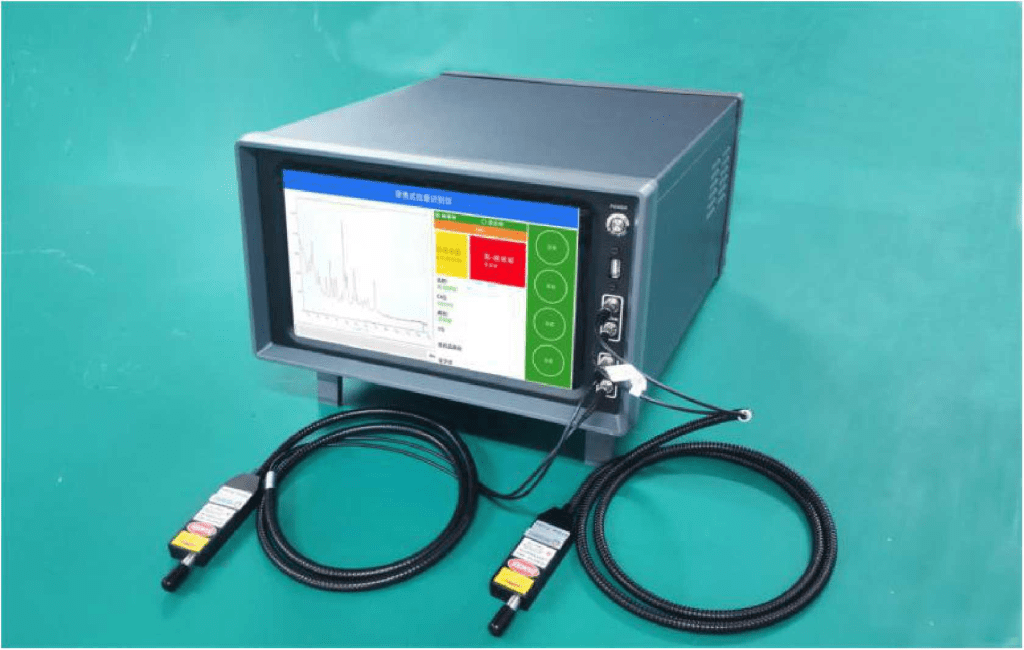
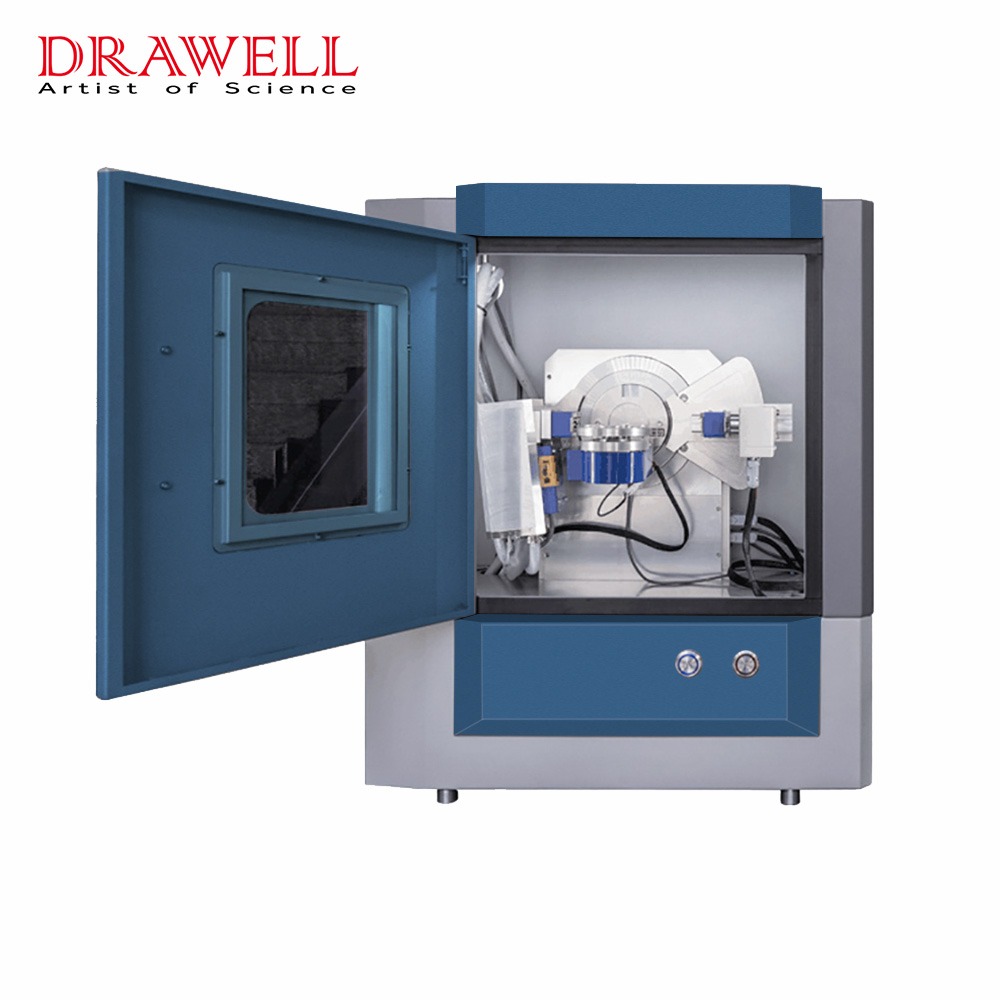
Related Products Recommendation

What Next?
For more information, or to arrange an equipment demonstration, please visit our dedicated Product Homepage or contact one of our Product Managers.