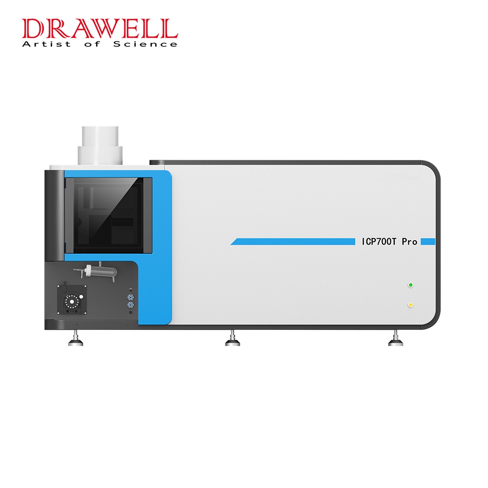
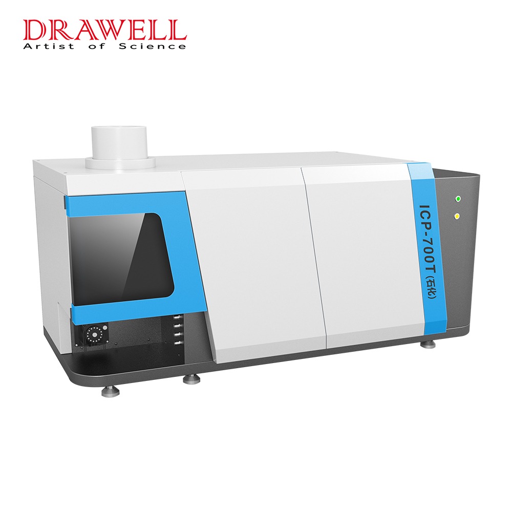
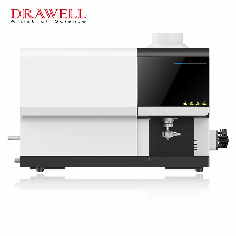
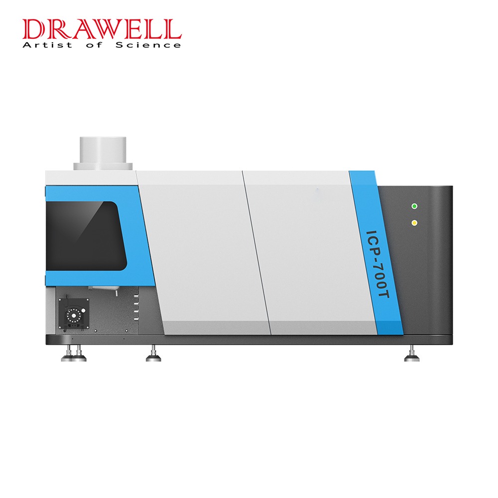
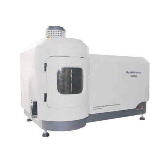
Inductively Coupled Plasma Optical Emission Spectroscopy (ICP-OES) is a powerful analytical tool that excels in multi-elemental analysis with high precision and sensitivity. Its applications in nanotechnology and material science have grown significantly, enabling breakthroughs in research, quality control, and product development.

Understanding ICP-OES
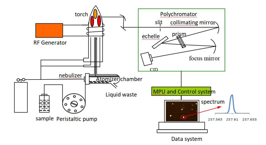
ICP-OES is an advanced analytical technique used to determine the elemental composition of a sample. It utilizes a high-temperature plasma to excite atoms and ions, causing them to emit light at characteristic wavelengths. These emissions are then measured to identify and quantify the elements present. Renowned for its precision, sensitivity, and ability to analyze multiple elements simultaneously, ICP-OES is widely applied in fields such as environmental science, nanotechnology, material science, and industrial quality control.
How ICP-OES is Applied in Nanotechnology and Material Science
1. Elemental Composition Analysis
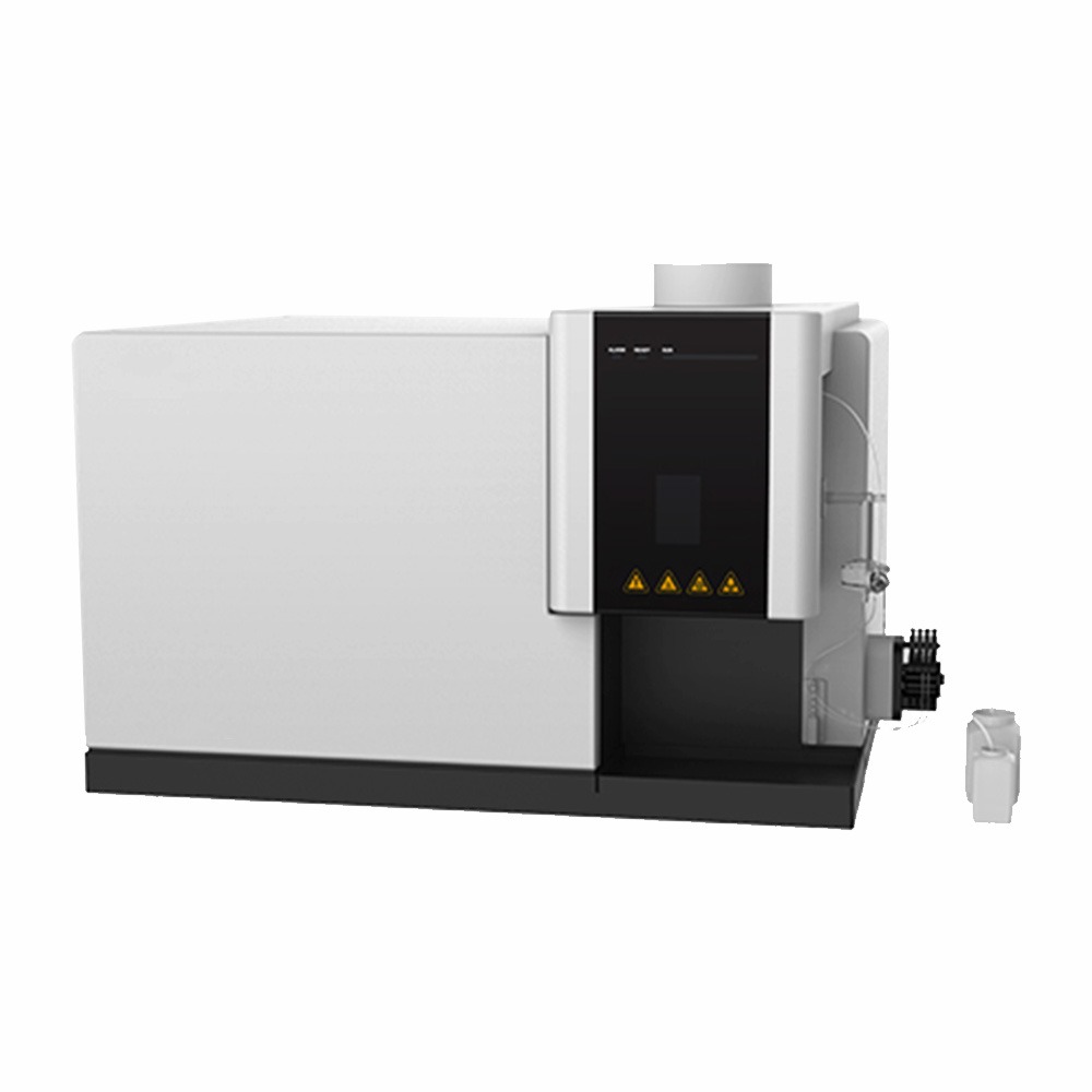
ICP-OES instrument is widely used to determine the elemental makeup of nanomaterials and advanced materials, crucial for their design and functionality.
Applications
- Nanoparticles: Quantifying metal content in metallic and metal oxide nanoparticles (e.g., Au, TiO₂).
- Quantum Dots: Measuring dopant concentrations to fine-tune optical properties.
- Alloys: Identifying minor and trace elements in advanced alloy systems.
Precise elemental data ensure material properties meet application-specific requirements, such as conductivity, strength, or reactivity.
2. Purity and Trace Element Detection
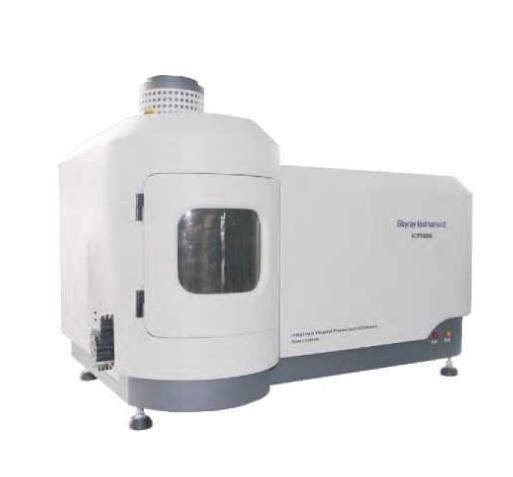
In both nanotechnology and material science, purity is critical to achieving desired performance. ICP-OES detects trace impurities that can compromise functionality.
Applications
- Verifying the purity of carbon nanotubes and graphene.
- Monitoring trace contaminants in high-purity metals and nanocomposites.
Enables the production of defect-free materials for high-performance applications like semiconductors and sensors.
3. Surface Modification Analysis
Nanomaterials often require surface modifications to enhance their performance, such as functional coatings or ligand attachments. ICP-OES is instrumental in evaluating these modifications.
Applications
- Quantifying metal coatings on nanostructures.
- Analyzing functional groups in biosensors and catalysts.
Ensures the uniformity and stability of surface modifications for applications in biomedicine and catalysis.
4. Quality Control in Manufacturing
ICP-OES supports quality assurance in the manufacturing of nanomaterials and advanced composites by monitoring elemental composition and process consistency.
Applications
- Ensuring consistency in nanoparticle production.
- Verifying doping levels in advanced ceramics and glasses.
Improves the reliability and performance of materials used in industries like electronics, aerospace, and energy storage.
5. Environmental Monitoring of Nanomaterials
With the growing use of nanotechnology, understanding the environmental behavior of nanomaterials is crucial. ICP-OES is used to study their stability, degradation, and potential environmental impacts.
Applications
- Measuring leaching of metals from engineered nanoparticles.
- Monitoring the adsorption of pollutants on nanomaterials.
Supports the development of eco-friendly materials and sustainable practices.
6. Advanced Material Characterization
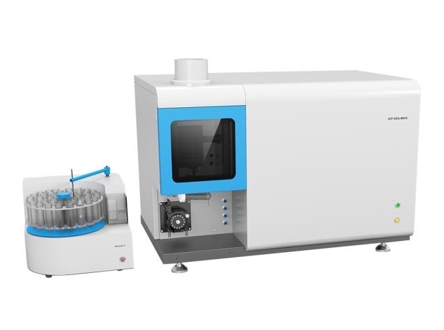
ICP-OES spectrometer aids in the characterization of innovative materials, including hybrid materials, polymer composites, and multi-phase alloys.
Applications
- Quantifying elemental distribution in complex matrices.
- Analyzing the interfacial composition of composites.
Facilitates the creation of materials with tailored properties for specific industrial and scientific applications.
Key Advantages of ICP-OES Applied in Nanotechnology and Material Science
- Multi-Element Analysis: ICP-OES can simultaneously detect and quantify multiple elements, making it highly efficient for characterizing complex nanomaterials and advanced materials.
- High Sensitivity: The technique offers excellent sensitivity, allowing the detection of trace elements, which is essential for controlling impurities in nanotechnology and material science applications.
- Wide Dynamic Range: ICP-OES provides accurate measurements over a wide concentration range, enabling the analysis of both trace and bulk elements in a single run.
- Robustness with Complex Matrices: The system handles diverse and challenging sample matrices, making it suitable for analyzing composite materials and multi-component nanostructures.
- Speed and Efficiency: Rapid analysis with minimal sample preparation ensures quick turnaround times, critical for research and industrial applications.
- Reproducibility: The technique delivers consistent and reliable results, which are vital for quality assurance in nanomaterial and material science studies.
- Cost-Effectiveness: Compared to more advanced techniques like ICP-MS, ICP-OES offers a balance of performance and cost, making it accessible for routine analyses.
- Small Sample Requirements: Requires minimal sample volume, preserving valuable or limited nanomaterial samples and suitable for high-cost or rare materials, common in nanotechnology research.
- Versatility in Sample Types: Accommodates liquids, powders, and digested solids, offering flexibility for various nanomaterial forms. ICP-OES is easily integrates into workflows involving dispersions, coatings, and bulk materials.
- Precise Stoichiometric Analysis: Determines the exact composition of advanced materials, such as quantum dots, metal oxides, or layered nanostructures and ensures consistency in synthesis and application.
Future Prospects in ICP-OES Applied in Nanotechnology and Material Science
This chart provides a concise summary of the anticipated advancements and their impact on nanotechnology and material science through ICP-OES.
| Prospect | Description | Impact |
| Enhanced Detection | Improved sensitivity to detect ultra-low element concentrations. | Enables analysis of smaller nanostructures and trace impurities. |
| Automation and AI | Integration of automated sample preparation and AI-driven data analysis. | Streamlines workflows, reduces errors, and accelerates analysis. |
| Real-Time Monitoring | On-the-fly process monitoring during material synthesis and fabrication. | Ensures quality control and dynamic optimization of production. |
| Miniaturization | Development of portable and compact ICP-OES systems. | Facilitates on-site and remote elemental analysis. |
| Multimodal Integration | Combination of ICP-OES with techniques like ICP-MS and Raman spectroscopy. | Provides comprehensive material characterization and deeper insights. |
| Sustainability | Energy-efficient plasma generation and reduced argon gas consumption. | Aligns with green chemistry initiatives and lowers operational costs. |
| Biomedical Applications | Expanded use in nanoparticle drug delivery, implants, and nano-coatings for medical devices. | Enhances material safety and performance in biomedical applications. |
| Advanced Material Studies | High-resolution analysis for new materials like 2D materials and metamaterials. | Supports innovation and characterization in cutting-edge material research. |
| Standardization and Sharing | Development of standardized data formats and cloud-based sharing platforms. | Encourages collaboration across research disciplines and global laboratories. |
In summary, the emerging applications of ICP-OES in nanotechnology and material science demonstrate its adaptability and indispensability. Through enabling precise elemental analysis, supporting quality control and fostering innovation, ICP-OES is driving advancements in these cutting-edge fields.

2.jpg)
